


Hardware
- Schematic Diagrams Of Satellite Equipment:
Passive SAT-splitter
This simple splitter allows to split IF signal coming from an LNB to two DVB-receivers. Using this splitter you should be sure that all the channels from received satellite are placed in one defined polarization and subband (i mean the low-band and the high-band of the Ku-band). But the high-band (when used 22kHz-tone) and horizontal polarization have higher priority. The splitter was developed as cheap alternative of twin-LNB, but anyway a twin-LNB is more universal and reliable. I am using three same splitters and i'm for the moment satisfied :)

Using example:
Assembling example:
H/V-Switch
Using example:
Schematic:
Self-made construction view:
22kHz-Switch
Using example:
Schematic:

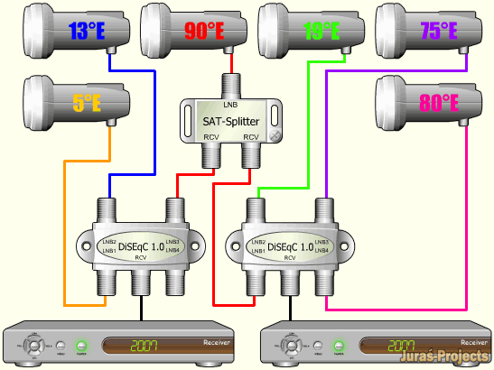
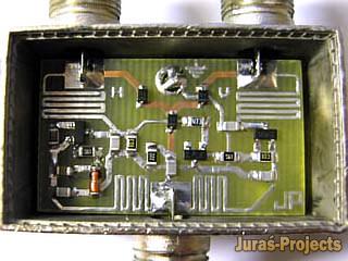
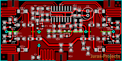
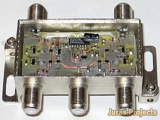
H/V+0/22kHz Combo-Switch

This is an attempt to combine together two well known kinds of switches, which are used in the practice of the satellite reception. The so called "Combo-Switch" was useful for obsolete receivers with only DiSEqC 1.0 level support and it solved the problem with more than four LNBs connection to one receiver. In fact, at the moment almost all receivers have a support of the full range of DiSEqC levels. Each input of the combo-switch will be active during its own condition. For example when the polarization is vertical (13V) and the subband is high (22kHz ON). Sure, you should consider features of broadcasting of satellites you are using (subbands and polarizations).

Using example:

Maximum capability using example:

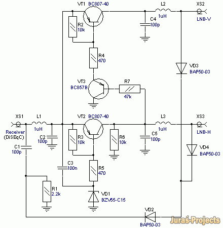
Schematic diagram:

PCB of Combo-Switch (P-CAD):
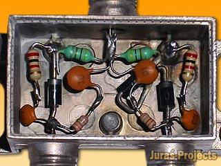
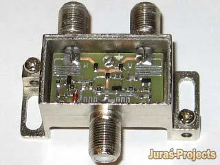
Example of manufacturing:
![]() Combo-Switch.pcb - Combo Switch PCB (PCAD 2004)
Combo-Switch.pcb - Combo Switch PCB (PCAD 2004)
DiSEqC 2.0/1.0 Switch schematic diagrams
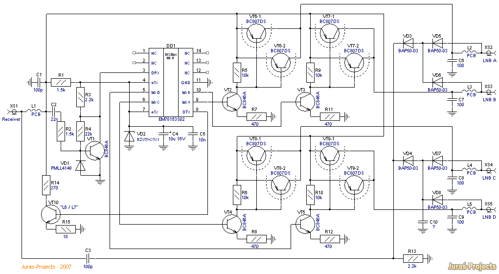
DiSEqC 2.0/1.0 Switch 4x1 schematic diagram using EM78153S02: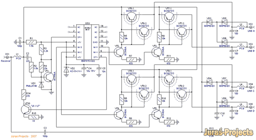
Enlarge
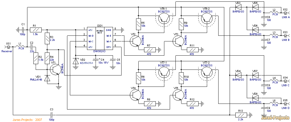
DiSEqC 1.0 Switch 4x1 schematic diagram using HS108N / DWS62K3:
Enlarge
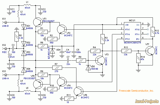
DiSEqC 2.0/1.0 Switch 2x1 schematic diagram using MC68HC908QT4 (Motorola):
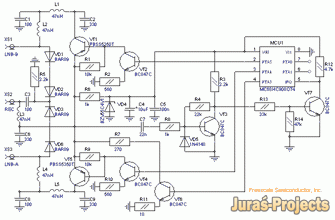
Enlarge
More info about some models of DiSEqC-switches is here.
Lumax LX-LST40 Single Universal LNB schematic diagram and pictures inside
I have disassembled this LNB to draw a schematic diagram of an LNB, since I couldn't find any schematic diagram of such device.

The LNB without plastic case:
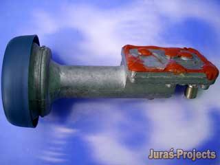
Is very hermetic... It's really hard to remove!

The LNB after some actions:
The back side of the top cap:
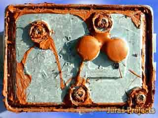
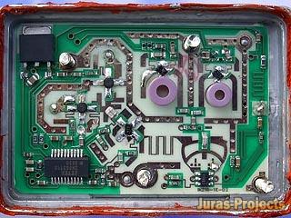
So, we can see a PCB inside the LNB chassis:
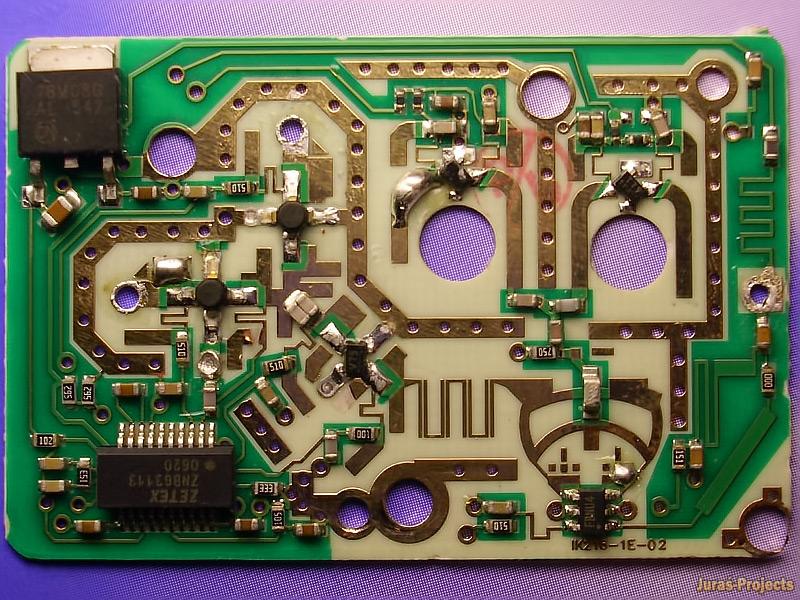
The PCB without the chassis:
Click to enlarge
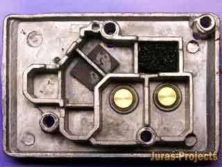
And the back side of the PCB:

Simplified schematic diagram of the LNB:
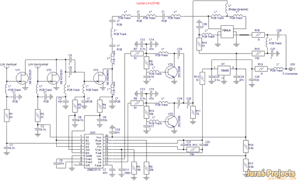
The most interesting thing is that the transistors (NE4210S01 from NEC) used in the first stage have typical noise figure 0.5-0.7dB depending on frequency and other conditions. At the same time the whole LNB's noise figure is marked as only 0.3dB! Fantastic? Take this fact into account when buying a new "super low noise" LNB.
![]() Download large picture of the schematic (12264 downloads)
Download large picture of the schematic (12264 downloads)
See also more pictures of another type of LNB (Pauxis DX-2200).
Please, do not distribute it at forums. The schematic diagram may contain discrepancies.
to be continued...